Now that you know about gates and registers, the basic building blocks of
digital logic, you're ready to start learning about how these functions are
actually implemented in electronic circuits.
Logic gate implementations
Some very early electronic computers implemented their logic gates using
relays.
A relay is a switch which is controlled by an electric current.
When electricity flows through the relay coil, it forms an electromagnet which
moves a simple switch to the opposite position.
An AND gate could be implemented by two relays in series (electricity has to
flow through both switches) while an OR gate could be implemented by two
relays in parallel (electricity can flow through either switch).
Inverters were accomplished simply by having the relay switch to the
"off" position, rather than "on," when energized.
Relays for digital logic were straightforward and easy to understand.
They also consumed a great deal of power and generated a great deal of heat
from the coils, they were slow (a relay takes a fair fraction of a second
to switch and settle) and they were prone to failure (over time, switches
would start to stick or not make good contact).
After relays, early computers used vacuum tubes.
Part of a vacuum tube is an "electron gun," which shoots a stream
of electrons through the vacuum.
Electrical charges applied to metal plates along the path of the electron
stream could deflect the stream to a different path.
Other plates would receive the electrons where they arrived.
Vacuum tubes could "switch" electric current much faster than relays
and were somewhat less prone to failure, although they still consumed lots of
power and generated lots of heat.
Electronics of all sorts took a great step forward with the invention of the
transistor.
A transistor is made of several materials with special electrical properties
such that, at the junction between materials, electron flow can be forced to
flow in special ways.
These materials, and their combinations, are called "semiconductors."
A small amount of current applied to one point in the transistor allows a
larger current to flow from another point in the transistor.
Logic gates could be implemented with a small number of transistors.
Transistors are faster than vacuum tubes, use a lot less power, produce a
lot less heat and last a long time.
As the manufacturing process for the transistors' materials developed, it was
just a simple logical step to combine more than one transistor in the same
component.
Then there were dozens of transistors on a single component, then hundreds,
then thousands, then millions as the technology and manufacturing processes
continue to improve.
These combined components are called "integrated circuits" or
"ICs."
These ICs range in complexity from the simple logic functions we've been
considering up to entire microprocessor systems.
Power consumption and heat generation continue to go down while speed
continues to increase.
Inside an IC there is generally a single square of semiconductor material that
has been built up in layers.
These squares are manufactured as a group on a larger "wafer" of
material and then separated into individual components.
The breaking of the large wafer into individual integrated circuit pieces has
given rise to the name "chip" as another term for IC.
The square of material is generally too small for humans to make connections
into the circuit, so the IC contains a relatively large package, with points
of electrical contact large enough to work with.
These contacts (called "pins" because they are often small rods of
metal designed to press into a socket or circuit board) are connected to the
internal semiconductor circuit, and then the whole thing is sealed in a
package of plastic or ceramic to protect the internals.
There have been a lot of different technologies employed in making these
chips, giving rise to a lot of "families" of chips.
And within these families there can be hundreds of specific parts.
But to keep things simple we're going to start out with just one family, the
7400 series of TTL logic, and with just a single chip, the original 7400.
7400 series TTL
TTL stands for "transistor-transistor logic."
A TTL logic circuit is based on some number of transistors to both perform the
desired logic function and present the output.
The first chip in this family has the part number "7400."
The 7400 contains four two-input NAND gates on one chip.
TTL logic chips are active components, requiring a connection to a power
supply in order to function.
This power supply should be five volts within a fairly close tolerance
(no less that 4.75V and no greater than 5.25V).
The chips consume some amount of electrical current at all times just by
being "on," and also generate some amount of heat.
 The 7400 chip is manufactured in a package called "DIP," which
stands for "dual in-line package."
This means that around a rectangular body of plastic, the chip has two rows
of pins, one on each long side of the rectangle, where the pins are all
arranged in a straight line.
Pins are spaced one tenth of an inch apart (0.1") in DIP components.
The 7400 has 14 pins (seven on each side).
For DIP parts with lower pin counts, including the 7400, the two rows of pins
are arranged to fall approximately three tenths of an inch (0.3") apart.
The 7400 chip is manufactured in a package called "DIP," which
stands for "dual in-line package."
This means that around a rectangular body of plastic, the chip has two rows
of pins, one on each long side of the rectangle, where the pins are all
arranged in a straight line.
Pins are spaced one tenth of an inch apart (0.1") in DIP components.
The 7400 has 14 pins (seven on each side).
For DIP parts with lower pin counts, including the 7400, the two rows of pins
are arranged to fall approximately three tenths of an inch (0.3") apart.
Pin-outs
Creating a logic function using 7400 series TTL involves finding the specific
parts that contain the gates you are looking for, connecting wires between
the pins of the chips that represent the inputs and outputs you need to use,
and connecting the chips to the 5V power supply at the appropriate power
supply pins.
This of course requires that you know what is "inside" particular
chips: the gates it contains, and the assignment of the pins to inputs,
outputs or power supply.
We use a diagram called a "pin-out" to map these pin meanings.
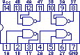
Each pin on a chip has a name and a number, as you can see from this pin-out
of the 7400.
On DIP parts, pin numbers start with "1" at a corner and proceed
down that side and back the other side.
The "orientation" of the part (which way you look at it to determine
pin 1) is usually indicated by a notch on the end that has the lowest- and
highest-numbered pins; on some parts there is instead a dot or marking on
the surface of the package adjacent to pin 1.
The 7400 contains four NAND gates.
Pins 1 through 3 are associated with the first gate, pins 4 through 6 are
associated with the second gate, and so on as indicated in the pin-out.
The names ("1A," etc.) tell you the specific function of a
particular pin.
When the internal function of the chip is simple like this one, it is common
to include the function as part of the picture.
Of course for more complex chips, this becomes impractical, and nothing is
drawn inside the rectangle of the chip; the behavior of the chip is then
described by truth tables or further text (still using the pin names to
describe the behavior).
The pin labeled "VCC" is the positive terminal of the
5V power supply, while the pin labeled "GND" is the signal ground
(the negative terminal of the voltage supply, and also the point from which
all voltage levels are measured).
These are not shown as connected to a particular gate because they are not
part of the logic function; rather they are the power supply that makes
any part of the chip work at all.
Logic levels
Back in our discussion of binary, I said that a logic "1" is
represented by the presence of voltage, and a logic "0" is
represented by the absence of voltage.
While this is a reasonable summary, it is time to get a bit more specific.
The output of a TTL logic gate represents a "1" by switching on an
electrical path through a transistor to the 5V supply.
If you measure the voltage of the output, relative to the signal ground,
you see a voltage which is near 5V, but reduced somewhat by flowing through
the transistor; the result is between 4V and 5V.
The TTL output represents a "0" by instead switching on a path
through a transistor to the signal ground.
If you again measure the voltage of the output, you will see 0V because there
is no path to the positive supply, but what you don't see is that there is
a separate path to the negative terminal.
That is, if you measured the output relative to the 5V supply, you would
see a voltage between -4V and -5V.
This is an important distinction: the output of a simple logic gate is never
actually "off."
(This is why I have avoided the terms "on" and "off" to
represent logic levels: "0" is not "off.")
One essential tool in digital logic is the logic probe, a
device which lets you see the logic level at a particular point in a circuit.
The logic probe has a small light that indicates when there is a "1"
(a path to the positive supply) and a separate light that indicates when there
is a "0" (a path to the signal ground).
When a circuit is off, neither light is lit; the signal in that case is said
to be "open" because there is no path to either the supply or
ground.
Since these are the characteristics of the outputs, it is only reasonable that
the inputs to TTL logic have similar characteristics.
For a logic "1," an input needs to see a path to the power supply,
indicated by a positive voltage above some minimum threshhold.
For a logic "0," an input needs to see a path to the signal ground,
indicated by a voltage at 0V or below some maximum threshhold.
(These threshhold values are part of the specifications of a chip, which I
will describe later in this course.)
Note that an unconnected input is neither a "0" nor a "1,"
and the level "seen" by the gate is undefined.
In practice, inputs on TTL logic gates are prone to "float" to a
logic "1" when unconnected, but this is not dependable so
don't count on it.
If you are not using all of the inputs on a chip, it is always a good idea to
tie the unused inputs to a signal (1 or 0) rather than letting them
float.
Signal propogation
When you set up the inputs of a logic gate, the output reflects the function
for those inputs.
But in the real world, this is not an instantaneous event.
There is some small element of time involved.
Suppose that an input started out at "0," then went to "1."
In reality there is no way that this can happen instantaneously.
There had to be some moment in time when the path to signal ground was turned
off (which also cannot occur instantaneously) and a subsequent moment in time
when the path to the power supply was turned on.
(We don't want these events to occur in the opposite order, because
then we would be creating a "short circuit" from power supply to
ground for the time interval when both were on; even if this event were not
long enough to damage the circuit it could still cause the power supply to
"glitch," dropping below 4.5V and causing your circuit to act
improperly.)
So there is some time interval, however small, when the input transitions
from being a clean "0" to being a clean "1."
The logic gate performs its function through a small series of transistors.
Each of these transistors takes an amount of time to react to its input and
switch its output.
The actual output stage of the gate is implemented as two transistors, one to
provide the path to the power supply for a "1" output and the other
to provide a path to the signal ground for a "0" output.
These transistors take some small interval of time to turn on or off, and
this time is added to the switching time of the internal logic transistors.
The time a logic gate requires for its outputs to correctly reflect the logic
function, measured from the point in time when the inputs are cleanly in
their new state, is called the "propogation delay."
These propogation delays are extremely short by human terms; the 7400 has
a propogation delay guaranteed to not exceed 22 billionths of a second
(and this is a slow chip by today's standards).
That is, whenever an input changes, the output is guaranteed to again correctly
reflect the NAND function in no more than 22 billionths of a second.
Obviously we can't see this time interval; when we work with logic gates, the
function appears to be instantaneous.
Since the time involved is so small it would be easy to ignore propogation
delays.
Unfortunately it can also be disasterous to a circuit design.
Consider a complex combinational logic function where gates feed into other
gates for several levels.
Not only do the propogation delays add up, but there can be unexpected results.
A chip specifies a range of time from the minimum delay possible to the
maximum; as signals flow through different gates, the propogation times could
differ, such that some signals within the circuit change faster than others.
When several parallel propogation delays feed into a common gate, this is
called a "race condition," because we cannot guarantee the
sequence of results.
While we know that the correct end result is reached after the sum of the
propogation delays, we have no assurance of what transitions could occur
before that time is complete.
The inputs could change from one configuration to another, both of which result
in the output in the same state, but because of the race condition within the
circuit there could be a brief time, undetectable by eye, when the output
changes to the wrong state.
Fan-out
TTL logic gates are, of course, designed to be combined in circuits.
Among things this means being able to connect a single output to multiple
inputs.
However each input consumes some amount of current from a signal in order to
detect its state.
As you add gates to a signal the current consumption increases, and the output
supplying the signal must be able to provide that amount of current.
The idea of supplying an output signal to multiple inputs is called
"fan-out."
I'll talk about current among the various chip specifications later in
this course, but actually TTL parts make it easy: one output may
drive up to ten inputs.
That is, the fan-out limit for TTL is 10 "TTL loads."
This is a fairly generous budget for most logic functions, and if you need to
connect a signal to more inputs than that, you can add buffer gates to gain
more TTL loads.
(For example, suppose you needed to drive 25 inputs with a single output.
Connect the output to five of the inputs, and also the inputs of two buffer
gates.
This means the output is driving a total of seven TTL loads, while each buffer
can drive an additional ten TTL loads.
The only trade-off with the buffers is they add their own propogation delay to
the circuit.
And if, in the section on logic gates, you were wondering why anyone would
ever have a need for a "do nothing" logic function such as a buffer,
this is one example.)
Let's try it
Now that our discussion of digital logic has finally moved off of the theory
and onto real-world logic chips, it must be time to try a circuit.
Let's actually build an S-R flip-flop!
For this project we're going to need the following items:
- A 7400 IC chip
- A breadboard with binding posts, such as (for example)
Jameco #20757
- A 5V DC regulated power supply, such as Jameco #155601
- A logic probe, such as Jameco #149930
- unstranded hookup wires (cut from 22 AWG wire such as Jameco #36791)
(If you are serious about learning this topic, it is worth your time to try
following this section with real hardware rather than just skimming the text.
Except for the chip, costing less than a dollar, these are useful items for
you or your school to own as part of the Computer Engineering Challenge.
The total cost for the items listed is less than $60.)
Note that if you have one, you can use a 74LS00 for this experiment instead
of a 7400.
I'll talk about what that distinction means in the next section.
The breadboard is an easy way to experiment with digital logic circuits,
because it is designed to accept DIP ICs, connector wires and many related
components.
Using the logic probe allows us to see what the circuit does, without having
to (yet) add the complexity of other components for displaying results.
Step 1: Hook up the power.
If your power suppy has a connector on the end, like the one I suggested
does, cut it off.
(This is for experimenting, not plugging into someone else's circuit.
Just make sure the supply is not plugged in when you cut it, because
your cutters will cause a short circuit.)
This leaves you with two stranded wires (made up of many finer wires twisted
together).
One of these wires is the positive terminal and the other is the negative
terminal.
Attach the positive wire to the red binding post on the breadboard (red is
used to indicate power) and attach the negative wire to the black binding
post.
(Not sure which wire is positive?
Use a multimeter if you have one... or else just guess because we'll
check it in a moment.)
Attach the red and black power clips from the logic probe to the matching
posts, so the logic probe has power.
Plug in your power supply.
At this point touching the tip of the logic probe to the red post should
cause the "high" or "1" light to light, and touching
the black post should cause the "low" or "0" light to
light.
If the logic probe doesn't work, your power supply either isn't working or
you have the terminals reversed.
Don't proceed until the logic probe agrees that red is 1 and black is 0.
Once you have that settled, unplug your power for now.
Step 2: Draw your circuit diagram.
We want to build an S-R flip-flop; our final logic diagram for that in the
last section was:
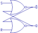
At this point we see a small catch, which is that the diagram needs two NOR
gates, but our 7400 instead contains four NAND gates, and I have not yet
introduced any part that contains NOR gates.
(There are such parts, of course, but for the moment we'll stick with just
the 7400.)
Fortunately, by this point you are comfortable changing logic diagrams by
applying DeMorgan's Theorem (right?), so it takes you very little time to
update the diagram again to look like this:
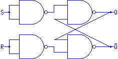
We can use a NAND gate as an inverter, by tying the inputs together.
Make sure you understand this diagram!
If you don't see how these two diagrams are equivalent functions, study them
and their truth tables until you "get it," because these sorts of
manipulations are common in digital electronics.
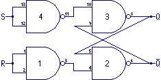
Step 3: Assign components.
This is the point where you figure out the components that will be used to
realize your logic function.
Of course we only have one type of component at the moment, and the four gates
we need happen to match the four gates offered by our component, so we are
really only assigning gates within the chip.
All four gates are the same so it doesn't matter which chip gate is which
diagram gate, but for simplicity, let's assign the gates so that the positions
of the NAND gates in the pin-out and in the logic diagram are the same.
We then mark our logic diagram with the identifier of each gate and the number
of each pin... like this:
Step 4: Wire the circuit.
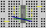
Place the 7400 in the breadboard, so the chip straddles the dividing line
between lines of connection points.
(There should be four open holes extending away from each hole where a
pin of the chip was inserted.)
Insert a jumper wire, with about a quarter inch of insulation stripped from
each end, in the breadboard to connect any two pin numbers where there is a
connection in your diagram.
In this particular diagram, then, the connection list would be:
1-2; 3-4; 5-8; 6-9; 10-11; 12-13.
Insert the end of the wire in one of the open holes extending from the
appropriate pin number (remembering how the pins are numbered).
Note that when pins are adjacent (like 1-2), it is easier to just strip the
insulation off a length of wire, around three quarters of an inch, and bend it
in a horseshoe shape as your connection; there shouldn't be any uninsulated
wires crossing such a connection that might cause a short.
 Step 5: Wire the power.
Usually a breadboard with terminal posts will also have power bus strips that
run along the outside of the component connection holes.
Attach jumper wires from the terminal posts to the matching power bus strips.
Then add a jumper from the positive power bus to pin 14 (the VCC
pin) and from the ground bus to pin 7 (the GND pin).
Step 5: Wire the power.
Usually a breadboard with terminal posts will also have power bus strips that
run along the outside of the component connection holes.
Attach jumper wires from the terminal posts to the matching power bus strips.
Then add a jumper from the positive power bus to pin 14 (the VCC
pin) and from the ground bus to pin 7 (the GND pin).
Step 6: Set the inputs.
Connect two jumper wires, longer than needed, from the ground bus to pins 1
and 13 (each of which already has a connection to the next pin).
These are your R and S inputs, each set to "0."
The jumpers need to be long enough to also reach your power bus when you want
to set them to "1."
Step 7: Power it up.
Plug your power supply back in.
Use your logic probe to first make sure that pin 14 shows a "1" and
pin 7 shows a "0" to make sure the chip is properly powered.
(If you reversed the power to the chip, it might get hot and/or burn out.
This is not the lesson you're trying to learn here!)
Also probe pins 6 and 8.
We don't know which way the flip-flop will "wake up," but we know
these two pins should be at opposite states.
Step 8: Test the circuit.
If you move the pin 13 jumper to the power bus and then back to the ground bus,
the logic probe should then see a "1" at pin 8 ("Q") and a
"0" at pin 6 ("/Q").
Similarly, if you move the pin 1 jumper to the power bus and then back to the
ground bus, the logic probe should then see a "0" at pin 8 and a
"1" at pin 6.
Try this a few times to prove that your circuit is working properly.
If the circuit doesn't work, it's a fair bet that your circuit is wired
incorrectly somewhere.
Other possible sources of difficulty are a damaged IC (especially if this part
has been used by others before you) or a bad power supply (if possible, check
it with a multimeter; a logic probe can tell you if there is voltage but not
whether it is a good 5V level).
Diagnosing a non-functioning circuit is a good exercise, because it will
certainly come up again in the course of the Computer Engineering Challenge.
Once you have a working circuit, it might be worthwhile to ask someone else
to make a change to the circuit (move or remove a wire... except don't mess
with the power and ground connections, since those could damage the part)
and then let you see if you can find out what is wrong and make it work again.
But at any rate, at this point you've actually built a working digital
electronics circuit.
And for any function that you can figure out that can be realized through
some combination of NAND gates, you know how to build it.
And once you know the details of other chips, you'll be able to do even more.
Next: Data Sheets
Previous: Registers
Copyright ©2003-2006, Mark Bereit. All rights reserved.
|