Now that you have seen how to turn a logic diagram into a working circuit,
and know about a number of useful logic chips, it's time to look at drawing
schematic diagrams... and also time to look at a number of other useful
components besides chips that can help make up digital electronic
circuits.
Schematic diagrams
In an earlier section we started with a logic diagram of an S-R flip-flop,
then assigned gates from a chip and filled in the pin numbers.
That "marked-up" version of the logic diagram was almost a complete
schematic diagram.
A schematic diagram is a drawing (however complex) which fully describes an
electrical circuit.
All the electrical components and their interconnections are represented.
A schematic diagram tells you how to build a circuit and how to check it.
In order to do much with digitial electronics, you will need to be able to
draw schematic diagrams and to read schematic diagrams created by others.
Every electrical component within the circuit is represented as a symbol on
the schematic diagram, or sometimes more than one symbol.
Each unique instance of a component is given a circuit-specific name, called
a "designator" so you have a way of referring to that component.
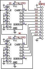
For example, imagine that your circuit contains two 74LS193 binary counter
chips.
The chip's part number ("74LS193") is not a sufficient term for
identifying the component because there are two of them.
By assigning one a designator of "U1" and assigning the other a
designator of "U2," you have a way of referring to the specific
component.
The schematic diagram includes the designator and the part number,
both located close to the component symbol.
When a component contains several distinct functional elements, like our
74LS00, it is often divided into a separate symbol for each element.
For example, the gate using pins 1 through 3 of the 74LS00 (a single
NAND gate) could appear as its own symbol in the schematic, just as it
did when we built our flip-flop.
All the elements of a chip share the same designator, but generally have
a suffix attached to describe the element.
If our 74LS00 had a designator of U1, the gate using pins 1 through 3
might be called "U1A" or "U1-1."
But whether one symbol or several, every pin of a component is shown, with
its pin name (if any) shown inside the symbol and its pin number (if any)
shown outside the symbol.
As with logic diagrams, straight lines connect the "pins" where
a connection is intended to exist.
(When building a circuit, these straight lines become the wires.)
Connection lines may go up, down, left or right regardless of the
"flow" of the signal; a convenient convention is to have signals
flow from left to right across the page but this is not a requirement
(and sometimes makes the diagram complicated; for parts which can flow
signals in two directions, such as the 74LS245, it is simply impossible!).
Lines are free to cross; this does not indicate a connection.
Rather, where the lines are connected, there is a closed dot to represent
the join.
(You may see a schematic, particularly older analog schematics, where
connection lines make a horseshoe-shaped "jump" over other lines
to indicate that no connection is intended.
However, this is an older convention which in most cases makes the schematic
harder to read.
Simply be sure in your schematics to make the connection dots heavy and
obvious so there is no question of the intent.)
Within a schematic, power connections are a recurring element.
Rather than show lines connecting all of these pin, you can use symbols to
indicate a connection to the "power plane" (usually a triangle
pointing up) or the "ground plane" (usually a set of horizontal
lines of decreasing size, looking something like a triangle pointing down).
When working with TTL logic circuits, the power plane is assumed to be
a 5V supply and does not require a label.
(In other, more complex systems where there are a variety of power supply
voltages, a label might appear next to the power symbol indicating just
which power is being used.)
These symbols for power and ground may be used anywhere a signal needs to
be connected to that level, not just for chip power supply pins.
Remember, it is not a good idea to let inputs "float;" every
unused input should be "tied" to a logic level.
An unconnected output, on the other hand, is perfectly all right.
However, in order to avoid confusing a deliberately unconnected output with
a forgotten pin, schematics sometimes use the convention of drawing a small
"X" at the end of an unused pin to indicate a deliberate no-connect.
Sometimes a signal (connection between pins) is important enough that it
warrants its own label.
This is a simple name placed immediately above a signal line.
Naming a signal has no electrical significance; it is simply a convenience
for human beings to describe the meaning of that signal.
There is also no reason that signal names have to agree with any of the pin
names to which they might be attached.
If you are familiar with computer programming, you might think of these signal
names as being comparable to local variable names within a function.
The sample schematic shown above also includes a connector.
There are a lot of different schematic symbols for different types of
connectors, but one common convention shows a series of open circles arranged
in the same general layout as the pins on the physical connector, each given
a pin number.
In the sample schematic, a twelve-pin straight line "header"
connector is the way signals get into and out of the circuit (a simple
eight-bit binary counter).
Given the schematic, you would be able to identify all of the components
(this list is called a "Bill of Materials"), and once you had these
components (and construction materials such as a breadboard and wires), you
would be able to assemble the intended circuit.
Further, given an assembled circuit and its schematic diagram, you would be
able to understand the function of the circuit and probe its behavior.
Integrated circuits
An integrated circuit is generally represented in a schematic as a box, with
pins arranged around the sides in any order that is convenient.
The name of the pin is inside the box; the line for the pin extends straight
out from the box opposite the name.
The pin number is outside the box, close enough to the line for the pin to
make clear which pin is indicated.
When an integrated circuit contains more than one functional block, it may
make the schematic clearer to split these blocks into separate boxes.
Alternately, if a circuit or section of the circuit corresponds to a logic
symbol, that logic symbol may be used instead of a box (since it is a clearer
representation of the function).
However, the power and ground connections for the chip need to be shown
somewhere; generally just one of the blocks shows the power pins and
their connections.
(In the earlier section where we built the S-R flip-flop circuit, none
of the NAND gates showed the power and ground connections; in a proper
schematic, these would have been indicated on one gate.)
Part designators for integrated circuits sometimes use "IC" as the
prefix (IC1, IC2, IC3...), but more often the letter "U" is used
(U1, U2, U3...).
Switches
So far in our discussions of digital logic circuits I have skirted around the
question of where input signals come from.
In our sample S-R flip-flop circuit the inputs were simply wires which we
connected to the power or ground bus as needed.
But a more practical signal source in a circuit is a switch.
Actually a switch is nothing more, electrically, than the wire we moved.
The simplest "on-off" switch makes an electrical path when
"closed" ("on") and breaks the path when "open"
("off").
This on-off switch is called a "single-pole, single-throw" switch
(SPST) because there is one electrical path (single pole) and only one setting
in which the path is closed (single throw).
Another useful switch is the SPDT (single-pole, double-throw), which has two
different closed paths (from a common pole) depending upon the way the switch
is set.
We might have used the SPDT switch in our S-R flip-flop circuit.
However, it would have needed to be a "break-before-make" switch,
meaning (for example) that when sliding the switch, the path to power would
have to be broken before the path to ground was made.
Using a "make-before-break" switch would mean that sliding the
switch would cause a temporary short circuit (where both power and ground
were connected to the input, and hence to each other).
The SPST and SPDT switches are modeled on a slide or toggle switch (like a
standard light switch).
But a more common type of switch for digital electronic circuits is the
push-button.
A key on a computer keyboard is a good example of a push-button.
When you press down the key an electrical path is closed, but as soon as you
releasd the key a spring causes the button to move back to its normal position
and break the circuit.
This is called a "normally open" (N.O.) push-button; a button which
is "normally closed" (N.C.) is passing a signal in its normal
position and breaks the circuit when pressed.
All the push-buttons I'm talking about are called "momentary"
push-buttons, meaning they return to their normal state the moment you
release them; you may also see "push-on, push-off" buttons in a
catalog, but these are really just toggle SPST switches that look like the
momentary push-buttons.
Part designators for switches generally use a prefix of "S" (S1,
S2, S3...).
The standard schematic symbols for these different switches are shown below.
Resistors
In electronics, any component or even wire has a property called
"resistance," which describes the reduction of current experienced
by electricity flowing through that component.
A component built specifically to present a known amount of resistance is
called a resistor.
The schematic symbol for a resistor is a zig-zag line, generally having
three "points" on either side; the part designator prefix for a
resistor is generally "R" (R1, R2, R3...).
| Resistor |
 |
One use of a resistor in digital electronics is as a "pull-up."
Consider the use of an SPST switch, or a push-button, as an input to a
digital logic chip.
It's no good.
When the switch is open, the input is effectively unconnected, and you
already know that an unconnected input is an input you can't count on to
be in any particular state.
The solution is commonly to use the switch to create a path to ground (or
not, when the switch is open), and also have a resistor connecting the
input to power.
The resistor is said to "pull up" the signal when the switch is
open; however the current is weakened by the resistor to the point that
when the switch is closed, the path to ground is stronger than the path
to power and the input "sees" a "0."
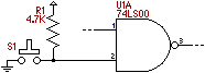
When the switch is open, the input sees a "1" because there is a
weak path to the power supply.
When the switch is closed, the direct connection to ground "wins."
Of course, the path through the resistor to power still exists, and that is
now connected to the ground, so some current flows through the reistor between
power and ground is wasted.
However, the pull-up resistor has a high enough resistance that this wasted
current is small.
In TTL logic, a pull-up resistor value of 4.7K is common; the wasted current
is around 1mA.
The pull-up technique can also be used when an input is fed by one or more
"open-collector" devices; like the switch above, an open-collector
output with a logic "0" provides a path to ground, but if no
outputs are "0," the pull-up resistor causes the result to be
"1."
Capacitors
A capacitor is a component which can hold a small amount of electric current,
like a very short-term battery.
When a current is applied to a capacitor the capacitor first "fills"
with current before allowing the current to pass through.
When current is removed, the charge stored within the capacitor discharges.
The schematic symbol for a capacitor is two parallel lines, or a line and a
curve, interrupting the line of a circuit.
Some capacitors are polarized, meaning they may only be used in a circuit
where one side is known to always be more positive (higher voltage) than the
other; in this case a plus sign marks the more positive side.
The designator for a capacitor generally begins with a "C" (C1,
C2, C3...).
| Capacitor |
Polarized
capacitor |
 |
 |
 |
 |
One important use of a capacitor in digital electronics is in smoothing out
glitches in a power supply.
When a logic gate changes, the current consumed by the integrated circuit
also changes by some small amount.
When a number of gates change at roughly the same time, the cumulative effect
of these changes can be a noticeable difference in the total circuit power
consumption; this in turn can have a short-term effect on the power supply,
causing the voltage to go above or below the intended voltage.
These effects also tend to be localized near the components where the changes
are occurring.
By placing a small capacitor near the power supply pin of each integrated
circuit the localized effects can be reduced.
This improves the reliability of the chip and decreases the chances that
the switching effects will cause problems for other chips in the circuit.
These "decoupling" capacitors are usually small values, such as
0.1µF or smaller, and are often drawn on the schematic close to
the power supply pin.
Sometimes the capacitors are shown in their own area of the schematic to not
further clutter the drawing, but this can obscure the intent, which is to
place the capacitors close to the parts they protect.
Semiconductor components
There are a number of components made of semiconductor materials, just like
integrated circuits are, for doing basic tasks.
The best-known is, of course, the transistor, a component
where a signal at one pin switches a signal between other pins.
An NPN transistor takes a small current of a positive voltage at a pin called
the "base" in order to let a different current (possibly larger
and/or a higher voltage) pass between a pin called the "collector"
(more positive) and the "emitter" (more negative).
The base current also flows through the emitter, so the emitter is generally
a path to the signal ground shared by both signals.
A PNP transistor takes a negative signal at the base to let a different
current pass between the collector (this time more negative) and the emitter
(this time more positive, but still common between the two signals).
There are other types of transistors with different symbols, but the NPN and
PNP types are the most common in digital logic.
One application for transistors in digital logic is to switch a current too
high for a logic chip to generate on its own, such as the coil current for a
relay.
| Transistors |
Diodes |
| NPN |
PNP |
Signal |
LED |
 |
 |
 |
 |
Another useful semiconductor component is the diode.
A signal diode is the electrical equivalent of a one-way street: current can
flow through a diode if the "anode" side of the circuit is more
positive than the "cathode" side, but if the cathode is more
positive, no current flows.
An interesting variant on the diode is the light-emitting
diode (LED), which works electrically like a signal diode, but has
the useful side effect that when current is flowing through the diode it
emits light.
The symbol for the LED is the same as a diode, except with one or two
zig-zag arrows moving away from the diode to indicate giving off light.
The standard prefix for a designator for a transistor on a schematic is
"Q" (Q1, Q2, Q3...) while the standard prefix for a diode or LED
is "D" (D1, D2, D3...).
Oscillators
One other component worth mentioning is an oscillator.
This is effectively a module like an integrated circuit which produces a
signal that changes state at a predictable rate.
The rate is generally quite high in human terms; a "slow"
oscillator would be 32,768 cycles per second (32,768Hz or 32.768kHz).
Many oscillators run at speeds above one million cycles per second (1MHz).
Since an oscillator is a single component module like an integrated circuit,
it is represented like an integrated circuit as a box with a few pins.
Typical oscillator modules have four pins; confusingly, many of them are
indicated by the manufacturer as having their pins numbered 1, 7, 8, and 14.
This seems bizarre until you observe that these modules were designed to
fit exactly into the corners of a 14-pin DIP socket, so these pin numbers
are based on the DIP package.
There are a number of ways to build an oscillator circuit using various
components such as resistors, capacitors, and logic gates or transistors,
with a part known as crystal providing the timing accuracy.
(In fact, the oscillator components contain just such a circuit, including
crystal, inside their package.)
However, it would take more conventional analog electronics than I am
prepared to include in this course to explain one of these circuits; the
easiest thing is to simply buy an oscillator component that does the whole
job for you.
Really big schematics
While you may not have thought of it yet, sooner or later you can reach a
point where a schematic is simply too large to fit on a single piece of
paper.
(Using larger sheets of paper only gets you so far.)
When the schematic becomes too big to reasonably draw on one sheet, you
need to divide the schematic across multiple pages (obviously) but still
indicate how connections cross the pages.
The simplest approach to describe is the off-page connector,
which is an arrow leading off the page and a name for the signal.
The assumption is that on one or more pages there are corresponding arrows
with the identical name.
A connection is assumed to exist between all off-page connectors with the same
name.
(If you have a computer programming background, think of the off-page
connectors as global variables.
The "scope" of these connectors is across the entire project.)
Some common symbols for the off-page connectors are the double arrows shown
here:
| Output |
Input |
 |
 |
While it is sometimes a convention to use the arrows pointing toward the
signal line to indicate an input to this sheet from another sheet, in fact
the arrows pointing outward can be used for outputs, inputs, bidirectional
signals or whatever.
A more hierarchical approach to the same problem is to divide your project
into functional blocks, where each block fits on a single sheet.
At its lowest level a sheet shows a block, where signals in and out of that
function are indicated with port pins.
The port pin is an arrow indicating a signal connection in or out of the
sheet (or both); as with the off-sheet connector, the pin has a name at
the opposite side from the signal line.
This sheet is then considered to be its own function block, which is included
in the larger project.
On some other sheet, there is a box like an integrated circuit whose
"pins" are the ports on the function sheet.
The box has a name that indicates the sheet containing the schematic details.
Each port is shown by name as a pin on the box, so that a signal that connects
to the pin is assumed to connect down into the port on the appropriate
sheet.
| Output |
Input |
Bidirectional |
 |
 |
 |
If you have a computer programming background, the sheet with the single
function is comparable to a code function and the ports are comparable to the
parameters of the function.
The other sheet that shows the function as a box is comparable to the code
that calls the function.
The scope of a port is local to that sheet, and accessible only through the
box representing that sheet on another sheet.
Now, experience in structured programming would seem to indicate that the
hierarchical approach and ports would be the preferred way to interconnect
sections of a schematic.
However, in practice this does not work as well as functions in
programming for a number of reasons.
First, in code you can call a function from several places, but in a schematic
it becomes confusing to use the function sheet more than once (because the part
designators can't repeat: if you used a sheet with U1 three times you would
have a circuit with three "U1" parts, or would connect the U1 part
three different ways, neither of which work).
Second, not every signal going into a functional block necessarily comes from
the same sheet, but apart from power and ground there is no provision for
"global" signals.
Third, not every good functional block fits nicely on a sheet; sometimes you
end up making fairly arbitrary divisions of a schematic not on functional
boundaries but on the basis of circuit size.
Some schematic capture tools address these issues with special syntax for
repeated blocks, for example.
There are projects whose size and complexity demands a better system of
managing interconnects than global off-page connectors.
But for hobbyist-sized projects, the off-page connectors are clearly the
easier way to span multiple pages.
(You will often encounter schematics where off-sheet connectors are used to
span pages, but the symbols used are the ones I showed for ports.
This is because these symbols are used both as ports and as off-sheet
connectors by different engineers.
A project actually using hierarchical ports will have at least one sheet
looking like a block diagram, showing the connection between sheets; if there
is no such diagram, then the project is using simple off-sheet connectors.)
Next: ...yet to be written...
Previous: 74LS00 Family
Copyright ©2003-2006, Mark Bereit. All rights reserved.
|